
JEE Prep Master

Reading mode

Text size

JEE Main 4 April 2024 Shift 2: Physics Question 19

Semiconductors and Electronic DevicesSingle correct option+4 / −1

Identify the logic gate given in the circuit:
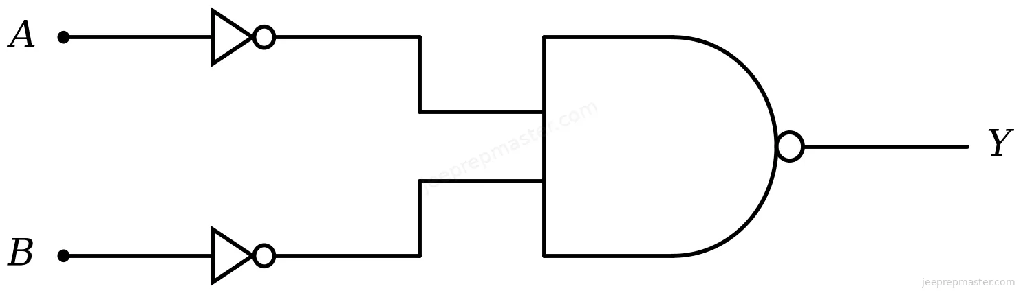
Input A and B each pass through a NOT gate, then enter an AND gate with an output inversion bubble, ending at Y.

Show answer and solution

Correct answer: Option 4

The two input inverters change AA and BB into A‾\overline{A} and B‾\overline{B}. The final gate is an AND gate with an inverted output, that is, a NAND gate.

Consequently Y=A‾⋅B‾‾Y=\overline{\overline{A}\cdot \overline{B}}. By De Morgan’s law, Y=A+BY=A+B, the Boolean OR operation. The entire circuit is therefore equivalent to an OR gate: option (4).

More Semiconductors and Electronic Devices questions

All 60 Semiconductors and Electronic Devices questions